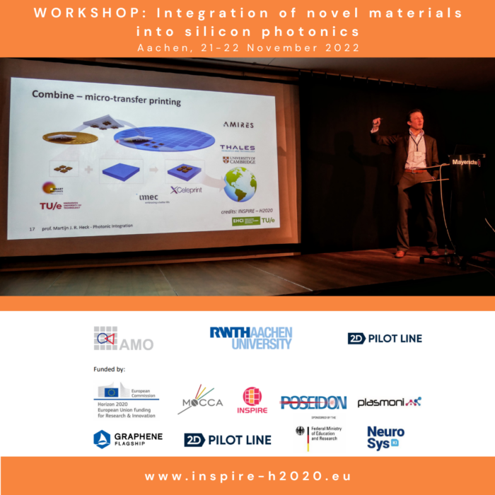
WORKSHOP: Integration of novel materials into Silicon photonics
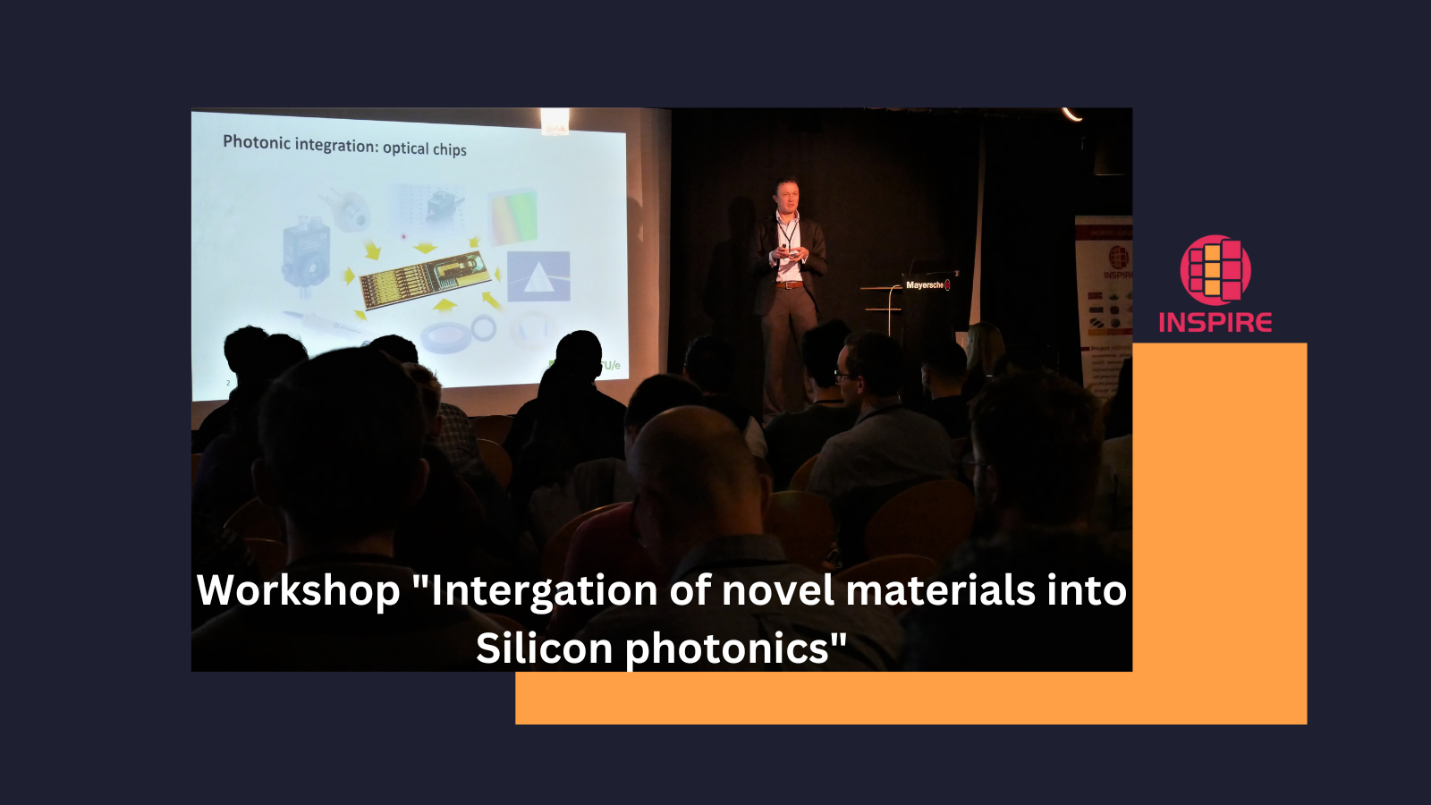
On 21-22 November, INSPIRE project supported the organisation of workshop titled “Integration of novel materials into Silicon photonics” in Aachen.
Martijn Heck has spoken about the challenges of each platform which INSPIRE comprises: InP has premium electro-optic performance, light sources and energy efficiency but small wafers don´t match those used in electronic production. SiN provides excellent optical performance, but lack of active electro-optic devices limits its deployment in many areas. Silicon CMOS is constrained by the use of nano-photonic waveguides compromising signal integrity.
INSPIRE realizes heterogeneous InP/SiN photonic integrated circuits, combining the best of each platform through wafer-scale micro-transfer printing.
Compatibility with open-access, generic, foundry manufacturing and the micro-transfer printing accuracy of 0,5 μm which is now within reach makes INSPIRE platform a scalable technology offering a clear route to volume production!
Thanks to AMO GmbH RWTHand Aachen University for the great organisation!